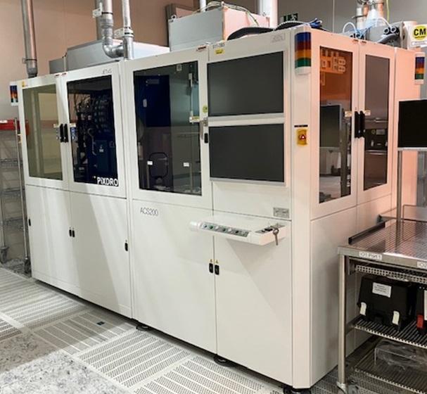
Other Wafer Fabrication Equipment
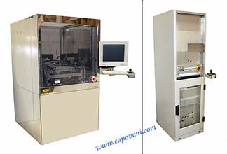
EV GROUP SMARTVIEW® BOND ALIGNER
2005 SmartView® Semi-Automated Wafer-to-Wafer Bond Aligner The EV Group (EVG) Smartview® Bond aligner and EV Group (EVG) 540 Wafer Bonder are used in the production of MEMs and in the emerging fields of 3D IC Packaging and Through-Silicon Via (TSV) interconnects.
A 3D integrated circuit (3D IC) is a single integrated circuit built by stacking silicon wafers and/or dies and interconnecting them vertically. This is achieved by persisly aligning devices on two silicon wafers and subsequently bonding them together. The result is they behave as a single device. By using TSV technology, 3D ICs can pack a great deal of functionality into a small “footprint.” This technology is not olny used in the production of MEMS, but also in the fabrication of CMOS image sensors, and memory devices.