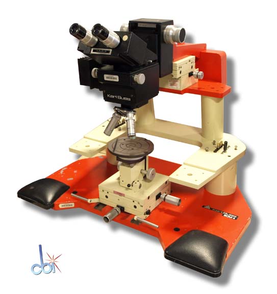
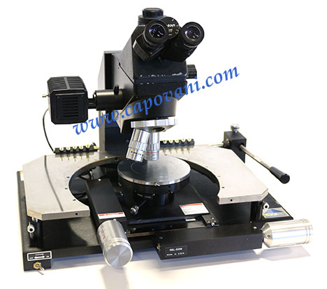
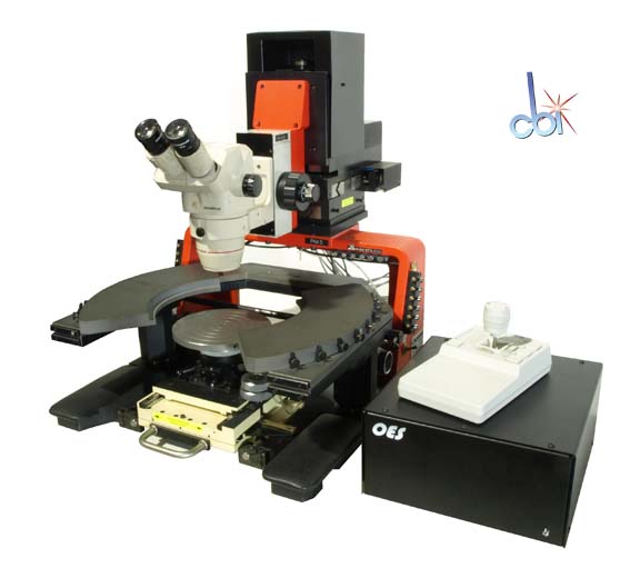
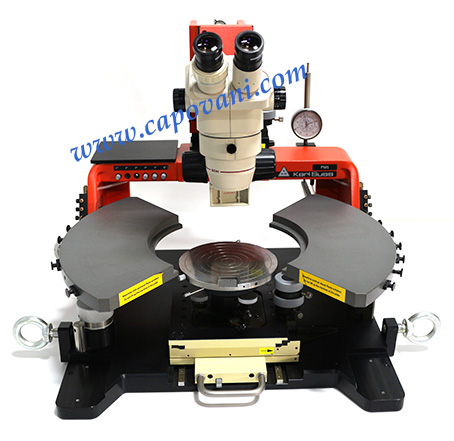
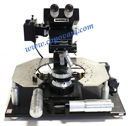
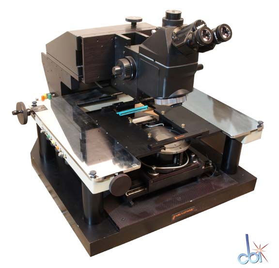
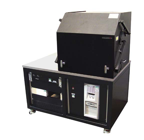
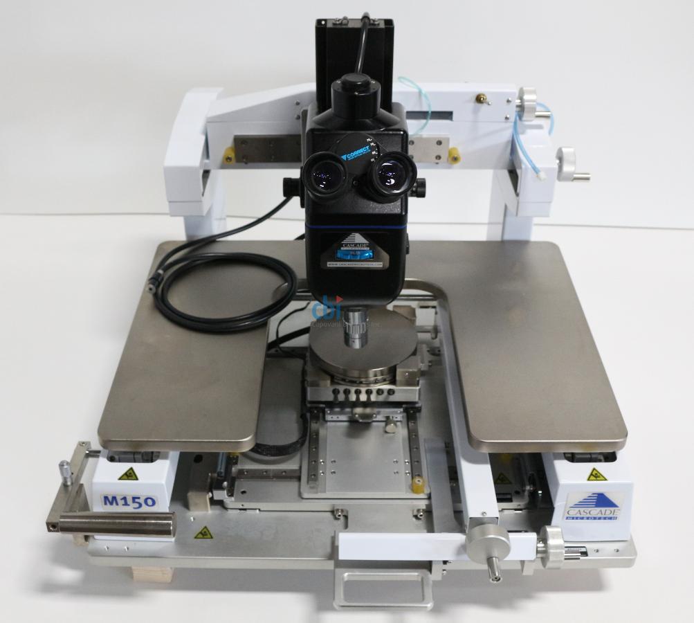
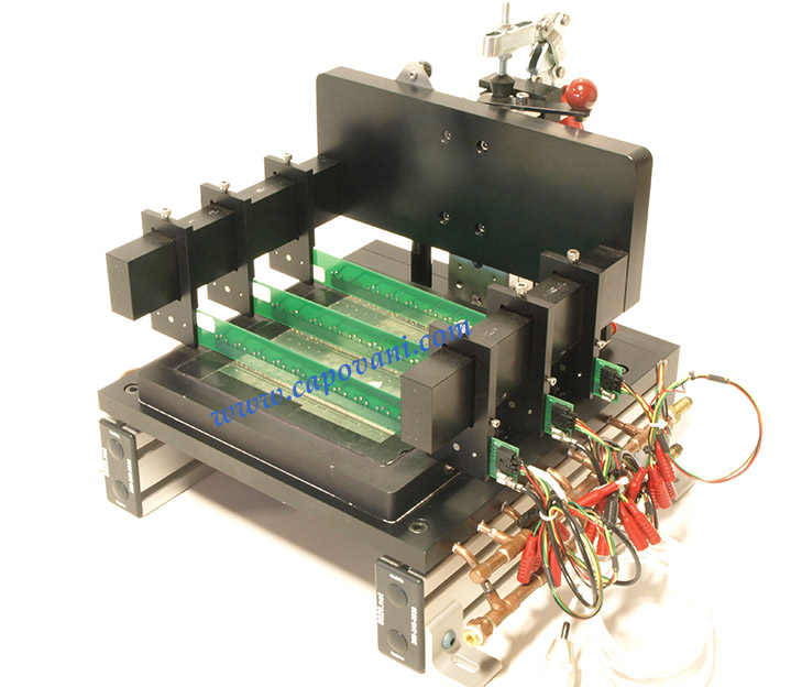
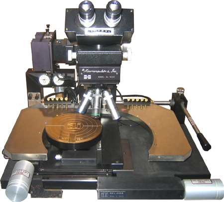
Wafer Testing & Probing
Wafer testing and probing equipment are critical tools used to assess the electrical characteristics of semiconductor wafers. These systems ensure high performance and reliability during semiconductor manufacturing processes.
-
-
-
-
-
-
-
-
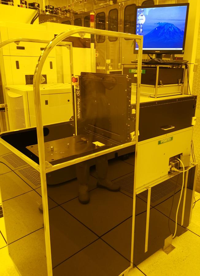
CDE ResMap 463-FOUP Resistivity Mapping Tool
CDE ResMap 463-FOUP Resistivity Mapping Tool
- For 300mm & 200mm Wafers
- Automatic Probe Head Selection
- This is a Donor Tool
- Please Inquire for Additional Details
-
-
-
-
Popular Manufacturers
Common Applications
semiconductor manufacturing
quality assurance
device reliability testing
material characterization
Frequently Asked Questions
What are wafer mobility testers used for?
Wafer mobility testers are used to determine the electrical mobility characteristics of semiconductor wafers, crucial for assessing material quality.
Why is electrical test equipment important in wafer testing?
Electrical test equipment verifies the functionality and integrity of semiconductor wafers by measuring their electrical properties, ensuring they meet required specifications.
What role does a wafer handling robot play?
A wafer handling robot automates the movement and positioning of wafers during the testing process, increasing efficiency and reducing the risk of contamination.
How does temperature testing affect semiconductor wafers?
Temperature testing is used to evaluate the performance and reliability of semiconductor wafers under different thermal conditions, critical for ensuring device stability.
Log in with your username/email address