Optics & Imaging
Optics and imaging systems are essential for examining and measuring semiconductor wafers. These systems ensure precise inspection to maintain high production standards.
-
-
-
LEICA/REICHERT MICROSCOPE, MANUAL WAFER INSPECTION
Manual Wafer Inspection MicroscopeMicroVision MVT 1080 Wafer Loader
-
NANOMETRICS CRITICAL DIMENSION COMPUTER
Critical Dimension Computer Large memory digital computer calculates line widths and provides statistics on in process wafer and photomasks.
-
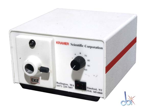
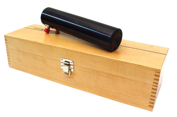
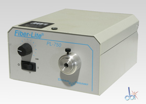
LEEDS FOSTEC FIBER OPTIC LIGHT SOURCE
Fiber Optic Light Source
Representative photo
These units are manufactured by Fostec and re-branded by different companies.The light source received may not be branded Fostec.
-
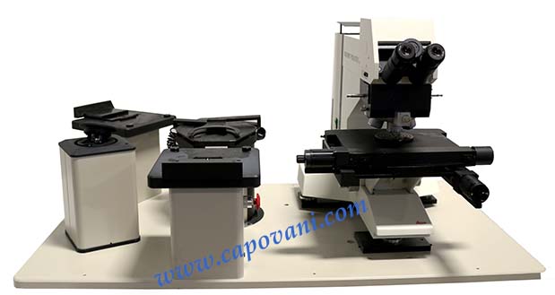
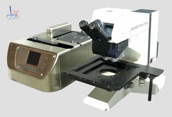
LEICA/REICHERT WAFER INSPECTION MICROSCOPE
Automated Wafer Inspection Microscope Brightfield/Darkfield/DIC With LEP motorized wafer transport system
-
-
-
-
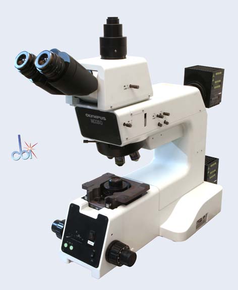
OLYMPUS SEMICONDUCTOR INSPECTION MICROSCOPE
Semiconductor Inspection MicroscopeReflected and Transmitted Light
-
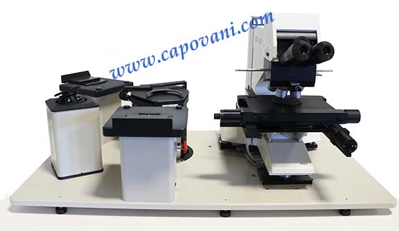
LEICA AUTOMATED WAFER INSPECTION MICROSCOPE
Automated Wafer Inspection Microscope Brightfield/Darkfield, DIC, With LEP motorized wafer transport system
-
Popular Manufacturers
Common Applications
Semiconductor wafer inspection
Defect identification
Film thickness measurement
Frequently Asked Questions
What are optical systems used for in semiconductor manufacturing?
They are used for precise inspection and measurement of semiconductor wafers.
Why consider surplus optics and imaging equipment?
Surplus equipment can offer cost-effective solutions without compromising on performance.
What should I verify when buying used optical systems?
Check calibration, condition, and compatibility with existing tools.
What types of optical systems are available?
Available systems include optical microscopes, defect inspection tools, and film measurement equipment.
Log in with your username/email address