Wafer Inspection Microscopes
Wafer inspection microscopes are specialized tools designed for detecting defects and analyzing wafers in semiconductor production. They enhance accuracy and reliability in quality control processes.
-
-
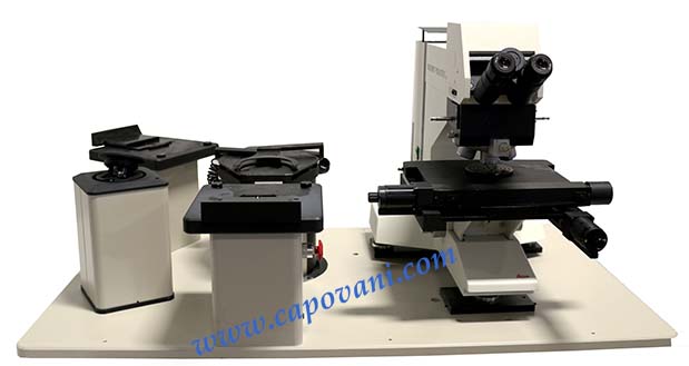
LEICA/REICHERT MICROSCOPE, MANUAL WAFER INSPECTION
Manual Wafer Inspection MicroscopeMicroVision MVT 1080 Wafer Loader
-
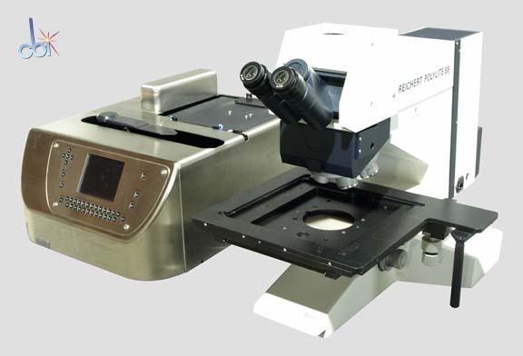
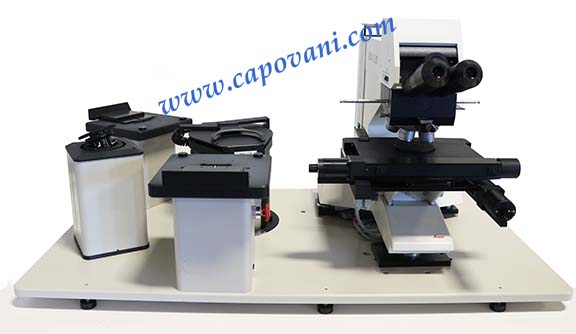
LEICA/REICHERT WAFER INSPECTION MICROSCOPE
Automated Wafer Inspection Microscope Brightfield/Darkfield/DIC With LEP motorized wafer transport system
-
OLYMPUS SEMICONDUCTOR INSPECTION MICROSCOPE
Semiconductor Inspection MicroscopeReflected and Transmitted Light
-
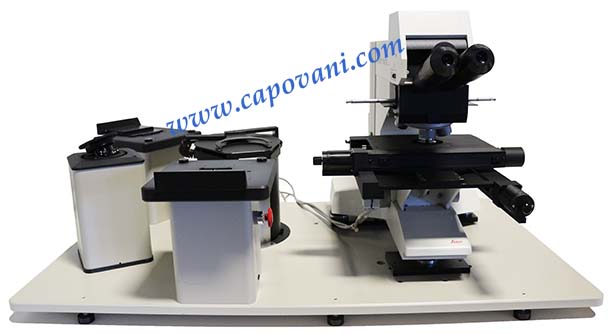
LEICA AUTOMATED WAFER INSPECTION MICROSCOPE
Automated Wafer Inspection Microscope Brightfield/Darkfield, DIC, With LEP motorized wafer transport system
-
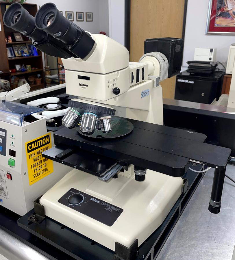
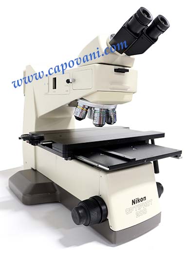
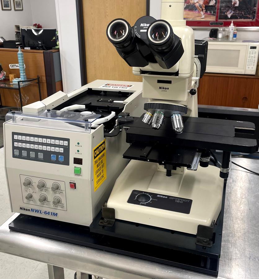
Nikon Optiphot-150S Wafer Inspection Microscope
Nikon Optiphot-150S Wafer Inspection Microscope
- 2.5X, 5X, 10X, 20X & 50X CF Plan Bright/Darkfield Objective Lenses
- Binocular Head with CFWN 10X/20 WF Eyepieces
- Wafer Stage for Use with Nikon NWL-641 Wafer Loader
- 12V/50W Lamphouse with Internal Illumination Transformer
- Nikon NWL-641M Wafer Loader & Wafer Transfer XYO Stage
- Macro Inspection Capability
- Also Available with Bright/Darkfield Objective Lenses
- Also Available with Ergo Trinocular Head and Color Camera
- Also Available without NWL-641 Wafer Loader
-

Nikon Optiphot 200
NIKON Optiphot 200 Wafer Inspection Stand, Including
- Focus Mechanism
- Interference Contrast Polarizer/Analyzer
-
LEICA/REICHERT WAFER INSPECTION MICROSCOPE
Automated Wafer Inspection Microscope Brightfield/Darkfield With LEP motorized wafer transport system
-
-
Nikon/Semprex Measuring Microscope
NIKON/SEMPREX Wafer Measuring Microscope
- 4 Position Turret
- NIKON MPlan 2.5X, BDPlan 10X, 20X & 40X Objective Lenses
- NIKON Binocular Viewing Head with 10X Widefield Eyepieces
- NIKON Vertical Illuminator with 12V/50W Halogen Lamp Housing
- Brightfield & Darkfield Channels
- Dual Iris Apertures
- NIKON Model UN Illumination Transformer
- SEMPREX Microscope Stand
- Specimen Stage 6” X 6.75”
- 2ea Mitutoyo 164-136 Digital Micrometers for XY Measurement
- 0-2” in X Axis & 0-1.5” in Y Axis; Resolution to 0.0001”
- Mitutoyo 534-223-1 Digital Micrometer for Height Measurement
- 0-1” in Z Axis; Resolution to 0.0001”
- Specimen Stage 6” X 6.75”
-
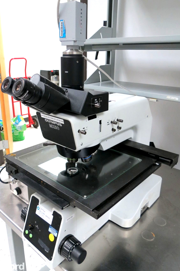
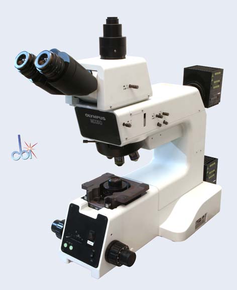
Olympus MX50 Wafer Inspection Microscope
OLYMPUS MX50A-F Reflected Light Microscope
- Five Position Motorized Turret with the Following Objective Lenses:
- OLYMPUS MPlanFl N 5X/0.15 BD
- OLYMPUS UMPlanFl 10X/0.30 BD
- OLYMPUS LMPlanFl 20X/0.40 BD
- OLYMPUS LMPlanFl 50X /0.50 BD
- OLYMPUS Trinocular Head with 2ea OLYMPUS WH10X Eyepieces
- OLYMPUS DBX Extension Tube with DIAGNOSTIC INST. 1.0X C Mount Adapter
- PIXELINK PL-B777U Solid State Camera
- Specimen Stage with 150mm X 150mm XY Travel
- OLYMPUS MX-LSH Lamp House with 12V 100W Halogen Lamp
- 100/115VAC 50/60Hz Input Voltage
- Five Position Motorized Turret with the Following Objective Lenses:
-
Nikon Optiphot-150S Wafer Inspection Microscope
Nikon Optiphot-150S Wafer Inspection Microscope
- 5X 10X, 20X, 50X & 100X CF Plan Brightfield EPI Objective Lenses
- Ergo Trinocular Head with CFWN 10X/20 WF Eyepieces
- Color CMOS Microscope Camera
- Wafer Stage for Use with Nikon NWL Wafer Loader
- 12V/50W Lamphouse with Internal Illumination Transformer
- Nikon NWL-641M Wafer Loader & Wafer Transfer XYO Stage
- Macro Inspection Capability
- Also Available with Bright/Darkfield Objective Lenses
- Also Available without NWL-641 Wafer Loader
Common Applications
Semiconductor production
Defect analysis
Quality control
Wafer evaluation
Frequently Asked Questions
What types of defects can wafer inspection microscopes detect?
These microscopes can detect surface defects, pattern defects, and particle contamination on wafers.
What is a common feature of surplus wafer inspection microscopes?
Surplus models often include advanced optical systems for high-precision inspection.
Are these microscopes suitable for all wafer sizes?
They are typically compatible with standard sizes, such as 200mm and 300mm wafers.
What brands of wafer inspection microscopes are available?
Brands like KLA Tencor and HSEB are commonly available in the surplus market.
Log in with your username/email address