Automatic Wafer Inspection Tools

Automatic wafer inspection tools are designed to detect defects and ensure quality in semiconductor wafers. They contribute to enhanced performance and reliability in semiconductor manufacturing processes.

  1. KLA 2367 "Escape" Bright Field Inspection Tool

    Automatic Wafer Inspection Tools

    KLA 2367 "Escape" Bright Field Inspection Tool

    BrightField Inspektionstool 25 cassette HW 200mmGEM/SECS and HSMS ModelEnable .12 , .62, .39 Picels

    ORS Upgrade done 

    Tool currently full installed at cleanroom (estimated time depending on areaneed)


    Sister tool available!

  2. KLA-Tencor 2138XP Brightfield Inspection Tool

    Automatic Wafer Inspection Tools

    KLA-Tencor 2138XP Brightfield Inspection Tool

    KLA-Tencor 2138XP Brightfield Defect Inspection Tool

    • 0.25µ, 0.39µ, 0.62µ Spot Sizes
    • For 150mm & 200mm Wafers
    • Model 2552UI User Interface
    • Denkenseiki Noise Filter
    • Please Inquire for Additional Details

Common Applications

Defect detection in semiconductor manufacturing

Quality assurance for 150mm wafers

Inspection of 200mm wafers

Automated wafer quality control

Brightfield inspection processes

Semiconductor defect analysis

Buying Guide

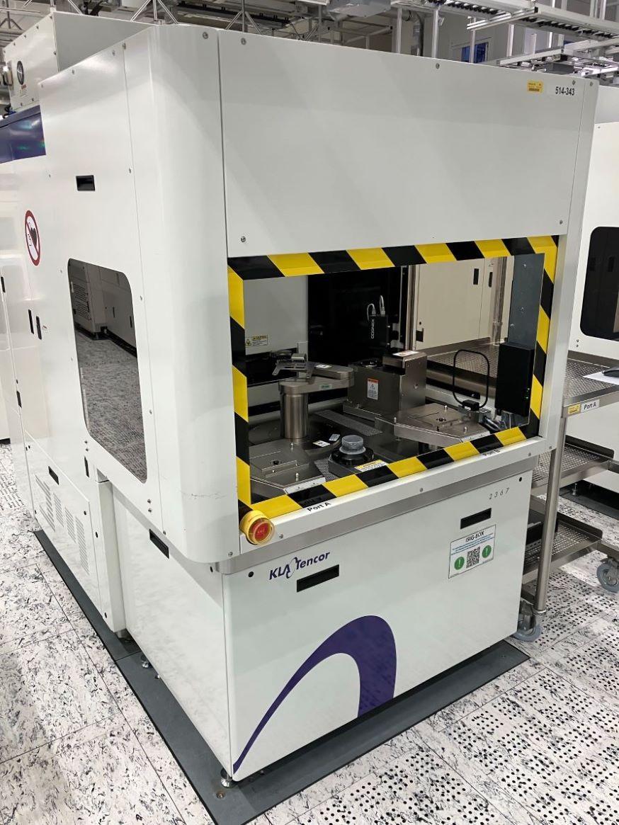
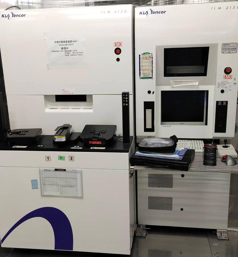
Automatic Wafer Inspection Tools Buying Guide

Selecting the right automatic wafer inspection tool is crucial for maintaining high-quality standards in semiconductor manufacturing. Consider the following aspects to make an informed decision:

Wafer size compatibility and inspection technology are key factors. Ensure that the tool accommodates your specific wafer sizes and supports necessary inspection techniques such as brightfield or darkfield.

  • Verify the configuration and options included in the tool, such as spot size and interface capabilities.
  • Assess the equipment's condition, ensuring it is suitable for long-term use before purchase.
  • Check for any upgrades or modifications like noise filtering systems or GEM/SECS compliance.
  • Ensure that documentation, including user manuals and interface guidelines, is available to facilitate seamless integration into your production environment.

Frequently Asked Questions

What do automatic wafer inspection tools do?
They identify defects on semiconductor wafers to ensure product quality.
Which wafer sizes are supported by these tools?
The tools typically support 150mm and 200mm wafers.
What brands of wafer inspection tools are available?
Brands such as Nikon and KLA-Tencor are commonly available.
How do these tools improve manufacturing processes?
They enhance the reliability and quality control of semiconductor production by detecting defects early.