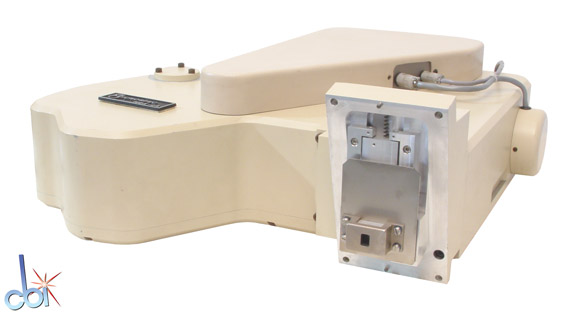
Scanning Electron Microscopes
Scanning electron microscopes are crucial for detailed inspection and analysis of semiconductor materials. They support precise defect detection and enhance production reliability.
-
-
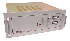
CPS SEM ELECTRON GUN POWER SUPPLY 30KV
Electron Gun Power Supply
CPS SEM Power Supply 6004
Common Applications
semiconductor inspection
defect detection
wafer analysis
Frequently Asked Questions
What are scanning electron microscopes used for?
They are used for high-resolution inspection and analysis of semiconductor materials to detect defects and ensure quality.
How do I choose a surplus scanning electron microscope?
Evaluate based on condition, specifications matching your needs, and available documentation such as manuals and maintenance logs.
Why is wafer scanning important in semiconductor manufacturing?
Wafer scanning ensures the detection of surface defects, which is crucial for maintaining production quality and yield.
What brands manufacture scanning electron microscopes for semiconductor use?
Brands like KLA are known for manufacturing specialized SEM equipment for semiconductor applications.
Log in with your username/email address