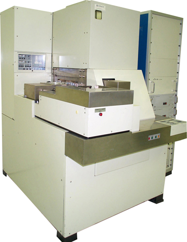
Critical Dimension Scanning Electron Microscopes
Critical Dimension Scanning Electron Microscopes (CD SEMs) provide high-resolution imaging essential for accurate dimension measurement in semiconductor manufacturing. These instruments enhance production efficiency and quality control by ensuring precise measurements.
Popular Manufacturers
Common Applications
semiconductor measurement
dimension verification
quality control
fabrication process monitoring
Frequently Asked Questions
What is a CD SEM used for?
A CD SEM is used for measuring the dimensions of semiconductor features with high precision.
Why are CD SEMs important in semiconductor manufacturing?
They ensure the dimensional accuracy of features, which is crucial for the functionality of semiconductor devices.
What are the benefits of buying a surplus CD SEM?
Buying surplus can offer significant cost savings while still providing the necessary measurement capabilities.
How do CD SEMs enhance quality control?
They provide precise and detailed imaging that helps in maintaining tight tolerances in semiconductor fabrication.
Log in with your username/email address